SemiconductorX > Chip Types > Sensor Semiconductors > Perception & Environment Sensors
Mature NodeMCUs
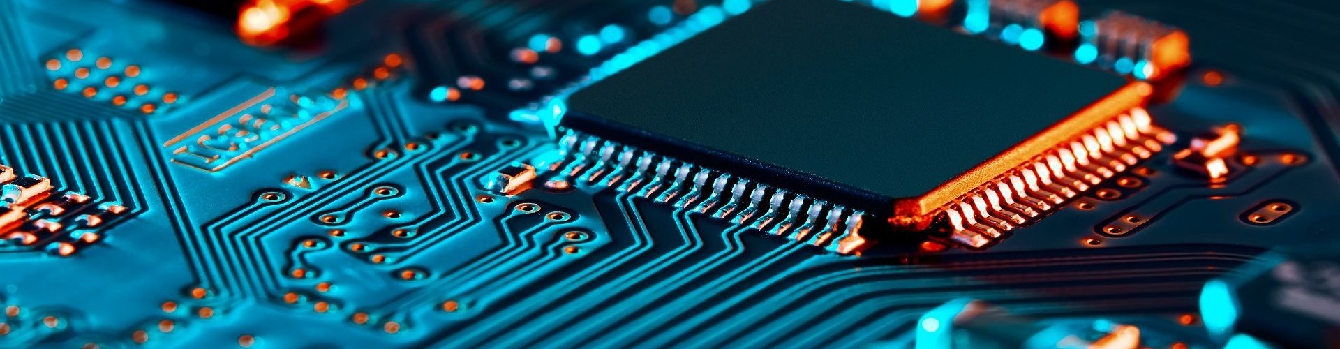
Perception and environment sensors — camera image sensors, LiDAR photodetectors and laser emitters, millimeter-wave radar transceivers, and ultrasonic transducers — are the physical interface between the AI-industrial system and the real world. Every autonomous vehicle, humanoid robot, and intelligent industrial platform depends on this semiconductor layer to observe its environment. Without it, no amount of inference compute, no trained model, and no planning algorithm produces a useful output. The perception sensor is where the physical world becomes data.
The supply chain for perception sensor semiconductors is structurally different from the mature-node MCU layer and from leading-edge logic. It spans five distinct semiconductor technologies — CMOS image sensors, compound semiconductor photodetectors (InGaAs, GaAs), vertical-cavity surface-emitting lasers (VCSELs), silicon germanium (SiGe) BiCMOS for mmWave radar, and piezoelectric MEMS for ultrasonics — each with its own materials, process, supplier concentration, and qualification pathway. The supply chain story is not one story; it is five parallel stories that converge at the vehicle or robot platform level.
For the system-level view — how perception sensors are integrated into ADAS and AV architectures, sensor suite design choices, and interface requirements — see ElectronsX: EV Sensors Overview. For the electromechanical sensing layer (voltage, current, temperature, position, force sensors in BMS, inverters, and humanoid robots) see Electromechanical & Control Sensors.
Perception Sensor Semiconductor Taxonomy
Each perception modality is enabled by a distinct semiconductor technology. The supply chain risk profile is completely different across modalities — Sony's CMOS image sensor dominance is a market concentration story; InGaAs APD scarcity for LiDAR is a compound semiconductor materials story; SiGe BiCMOS for 77GHz radar is a specialty process oligopoly story. Grouping them as "sensors" obscures the supply chain structure. The table below maps modality to semiconductor technology to supply chain character before going deeper on each.
| Sensor modality | Key semiconductor technology | Process character | Supply concentration | Primary bottleneck type |
|---|---|---|---|---|
| Camera (image sensor) | CMOS image sensor (CIS) — backside-illuminated (BSI) or stacked BSI with DRAM/logic | Specialty CMOS at Sony, Samsung, OmniVision — not standard logic foundry process; Sony uses proprietary stacked BSI process | Sony ~50-55% global CIS market share; dominant in automotive grade; Samsung second; OmniVision third | Market concentration + automotive qualification depth at Sony; Japan single-country risk; fab capacity allocation across automotive, mobile, and industrial |
| LiDAR (photodetector) | InGaAs avalanche photodiodes (APDs) and single-photon avalanche diodes (SPADs) for 1550nm; silicon SPADs for 905nm systems | III-V compound semiconductor (InP substrate + InGaAs epilayer) for 1550nm; specialty silicon for 905nm Si-SPAD arrays | Lumentum, Coherent (II-VI), Hamamatsu for InGaAs APDs; very limited supplier base at automotive grade | InGaAs compound semiconductor materials scarcity; 2-3 year automotive qualification cycle; no volume manufacturing precedent for LiDAR deployment scales |
| LiDAR (laser emitter) | VCSELs (vertical-cavity surface-emitting lasers) for flash LiDAR; edge-emitting lasers (EELs) for scanning LiDAR; distributed feedback (DFB) lasers for coherent LiDAR | III-V semiconductor (GaAs for VCSEL; InP for 1550nm EEL/DFB); MOCVD epitaxy; wafer-level testing critical | Lumentum dominant in VCSEL; II-VI/Coherent; ams-OSRAM; Princeton Optronics; very limited automotive-qualified VCSEL base | VCSEL wafer-level uniformity and reliability at automotive temperature range; MOCVD epi capacity; qualification for eye-safe power levels in automotive deployment |
| Radar (77GHz transceiver) | Silicon germanium (SiGe) BiCMOS — the only silicon-based process with sufficient fT (transit frequency) for 77GHz mmWave generation and reception | SiGe BiCMOS at 130nm-250nm; specialty process not available at all foundries; requires BiCMOS process capability alongside standard CMOS | NXP, Infineon, TI, Mobileye (EyeQ radar), Bosch — oligopoly of 4-5 suppliers with qualified automotive 77GHz SiGe process | SiGe BiCMOS process oligopoly; 77GHz antenna-in-package (AiP) integration is a specialty packaging challenge; automotive qualification at mmWave frequencies is uniquely complex |
| Ultrasonic (transducer IC) | Piezoelectric MEMS transducer + analog front-end IC; capacitive micromachined ultrasonic transducer (CMUT) emerging | MEMS specialty process; analog front-end on standard CMOS; transducer and IC often separate die | TI PGA460; NXP UJA; Elmos Semiconductor; Murata (transducer); relatively more distributed than other modalities | Lower concentration and lower strategic risk than other modalities; CMUT transition from piezo is the technology disruption risk |
| Camera ISP (image signal processor) | Digital logic SoC integrated into inference compute or as standalone ISP; handles demosaicing, HDR processing, noise reduction, serialization | Advanced CMOS logic; typically integrated into main inference SoC (NVIDIA Orin ISP, Tesla FSD ISP) or as discrete ASIC | Integrated into inference SoC for most platforms; standalone ISP: Renesas (ISP-less camera), STMicro; Mobileye integrates ISP into EyeQ | ISP tightly coupled to inference SoC — switching inference platform requires ISP re-optimization; adds to TSMC foundry dependency for integrated platforms |
CMOS Image Sensors — Sony's Structural Dominance
Camera image sensors are the highest-volume perception semiconductor in the automotive and robotics supply chain. A Level 2+ ADAS vehicle uses 8-12 cameras. A Level 4 robotaxi uses 8-12 cameras plus additional interior and driver-monitoring cameras. A humanoid robot uses 2-6 cameras for visual manipulation and navigation. At scale, camera image sensors represent the largest unit-volume perception semiconductor procurement across the entire AI-industrial ecosystem.
Sony Semiconductor Solutions holds approximately 50-55% of the global CMOS image sensor market by revenue and a significantly higher share in automotive-grade image sensors. Sony's dominance is not primarily a pricing or marketing outcome — it reflects a 20-year technology investment in backside-illuminated (BSI) sensor architecture, stacked sensor-plus-logic designs, and automotive-grade pixel process development that competitors have not replicated at equivalent performance. Sony's IMX series automotive image sensors — IMX490, IMX728, IMX623 — are the reference design for high-dynamic-range automotive cameras across most ADAS OEM programs globally.
| Supplier | HQ | Key automotive CIS products | Technology differentiation | Market position | Supply chain risk |
|---|---|---|---|---|---|
| Sony Semiconductor Solutions | Kumamoto / Nagasaki, Japan | IMX490 (surround view, HDR); IMX728 (high-resolution front camera); IMX623 (8MP front); IMX390 (legacy, widely deployed) | Stacked BSI: separate pixel wafer bonded to logic/DRAM wafer; enables pixel-level HDR processing and embedded memory; proprietary process not available to foundry customers | ~50-55% global CIS revenue share; dominant in automotive qualification depth; most ADAS reference designs specify Sony IMX | Japan single-country concentration; Kumamoto fab region (same prefecture as TSMC Japan fab); proprietary process means no second-source path; 2024 Kumamoto earthquake demonstrated regional risk |
| Samsung Semiconductor | Hwaseong, South Korea | ISOCELL Auto series; ISOCELL 4H (automotive HDR); targeting automotive market with ISOCELL family adapted from mobile CIS leadership | ISOCELL pixel technology; strong mobile CIS position (second globally); automotive qualification programs ongoing but behind Sony in depth and OEM design-win base | ~20% global CIS share; strong in mobile; automotive market penetration growing but limited qualified design wins vs. Sony | Lower automotive qualification depth than Sony limits substitution potential for programs already qualified on Sony IMX |
| OmniVision Technologies | San Jose, CA (USA); owned by Will Semiconductor (China) | OX03C (automotive surround, HDR); OX08B (8MP front camera); OX05B (5MP); strong in driver monitoring system (DMS) cameras | PureCel Plus-S pixel technology; uses TSMC and other foundries for manufacturing (fabless model); automotive-grade qualification across several product families | ~10-12% global CIS share; meaningful automotive presence particularly in DMS and rear-view; Will Semiconductor ownership creates US-China geopolitical exposure | Will Semiconductor (China) ownership creates CFIUS / export control exposure for US OEM programs; fabless model means TSMC foundry dependency; automotive programs may face sourcing restrictions |
| ON Semiconductor (onsemi) | Scottsdale, AZ (USA) | AR0820 (8MP HDR automotive); AR0233 (2MP surround); Hyperlux family targeting next-generation automotive HDR | Internal fab (IDM model for CIS — unusual); acquired Aptina (formerly Micron Imaging); automotive HDR focus with internal process control advantage | Smaller CIS market share but meaningful in automotive specifically; IDM model provides supply chain stability advantage over fabless competitors | Smaller scale limits R&D investment vs. Sony; automotive HDR performance gap vs. Sony IMX490/728 class remains in current generation |
The critical supply chain insight for automotive CIS is the stacked BSI architecture lock-in. Sony's stacked sensor design — where the pixel array wafer is bonded to a separate logic/DRAM wafer using Sony's proprietary Cu-Cu bonding process — enables pixel-level HDR processing and embedded frame memory that competitors cannot replicate without a similar proprietary stacked process. An automotive camera module designed for IMX490 cannot be redesigned for a Samsung ISOCELL equivalent without re-characterization of the full camera pipeline, new ISP tuning, and re-validation of HDR performance in all lighting conditions. The qualification lock-in for CIS is structurally similar to the MCU paradox — lower unit cost than MCU but substantial switching cost in engineering time and re-qualification.
LiDAR Semiconductors — Compound Semi Scarcity and the 905nm vs. 1550nm Split
LiDAR semiconductor supply is the most technically constrained perception supply chain — driven by compound semiconductor materials limitations at 1550nm and VCSEL uniformity challenges at automotive grade. The supply chain story divides cleanly along wavelength: 905nm systems use silicon-compatible detectors and GaAs VCSELs; 1550nm systems require InGaAs photodetectors and InP-based laser sources that live entirely in the specialty compound semiconductor world.
The wavelength choice is not primarily a performance preference — it is a materials and supply chain choice with major downstream implications. 905nm silicon SPADs and GaAs VCSELs can be manufactured on relatively accessible processes with broader supplier bases. 1550nm InGaAs APDs and InP edge-emitting lasers require III-V compound semiconductor expertise concentrated at a handful of suppliers globally, with 2-3 year automotive qualification cycles and no established volume manufacturing base at LiDAR deployment scales.
| LiDAR wavelength | Detector technology | Emitter technology | Key suppliers | Supply chain character | AV/robot program examples |
|---|---|---|---|---|---|
| 905nm | Silicon PIN photodiodes; silicon SPADs (single-photon avalanche diodes); Si APDs — manufacturable on modified CMOS processes | GaAs edge-emitting pulsed lasers; GaAs VCSELs for flash LiDAR — standard III-V process, broader supplier base than 1550nm | Detector: Broadcom, STMicro (Si SPAD arrays); Emitter: Lumentum, ams-OSRAM, II-VI/Coherent (GaAs); LiDAR module: Velodyne legacy, Innoviz, Luminar (905nm variant) | More accessible supply chain; GaAs VCSEL supplier base overlaps with consumer 3D sensing (Face ID) — larger volume production base; silicon detector compatible with standard fab processes | Mobileye RoboTaxi (EyeQ + Luminar 905nm); Continental HRL131; Bosch LiDAR; most production ADAS LiDAR (Valeo SCALA, Continental) |
| 1550nm | InGaAs APDs (avalanche photodiodes) on InP substrate; InGaAs SPADs for photon-counting; requires III-V compound semiconductor process — not silicon-compatible | InP-based edge-emitting lasers; distributed feedback (DFB) lasers for FMCW/coherent LiDAR; fiber-amplified MOPA architectures | APD: Lumentum, Coherent (II-VI), Hamamatsu, Voxtel (now Argo AI internal); Emitter: Lumentum, II-VI/Coherent, POET Technologies; LiDAR module: Luminar Iris (1550nm), Waymo custom, Aurora | Highest supply chain risk of any perception sensor semiconductor; InGaAs APD supply is the primary LiDAR scale-up bottleneck; 1550nm is eye-safe at higher power (enables longer range) but the compound semi supply chain has never been stressed at automotive volume | Luminar Iris (Volvo, Mercedes, Nissan); Waymo 5th-gen (custom 1550nm); Aurora (1550nm for Peterbilt robotruck) |
The InGaAs APD supply chain is SX's identified Wave 2 bottleneck — the perception sensor constraint that will become binding as AV and robot deployments scale beyond current pilot fleets. InGaAs APD wafers require InP substrates grown by HVPE (hydride vapor phase epitaxy), followed by InGaAs epilayer deposition by MOCVD, followed by APD device processing in a specialty III-V fab with avalanche multiplication region engineering. The entire chain — InP substrate, MOCVD epi, device fab, automotive qualification — is concentrated at 3-4 suppliers globally with combined capacity that was sized for telecom and scientific applications, not automotive volume. As LiDAR-equipped vehicle production scales from tens of thousands to hundreds of thousands of units per year, the InGaAs APD supply chain will face the same structural stress that SiC substrates faced in 2021-2023 — a compound semiconductor materials bottleneck with a 3-5 year expansion timeline.
VCSEL Supply — From Face ID to Automotive LiDAR
Vertical-cavity surface-emitting lasers (VCSELs) are the laser emitter technology for flash LiDAR and structured light sensing. The VCSEL supply chain was fundamentally reshaped by Apple's Face ID launch in 2017 — the first consumer product to require VCSELs at tens of millions of units per year. That volume signal drove Lumentum, II-VI (now Coherent), and ams-OSRAM to invest in VCSEL wafer capacity that now provides the production base for automotive LiDAR emitters.
The automotive LiDAR VCSEL requirement differs from mobile 3D sensing in three critical dimensions: operating temperature range (-40 to 105C vs. 0 to 70C for consumer), pulse power density (much higher peak power for long-range LiDAR than for face unlock), and reliability lifetime (15-year automotive vs. 3-5 year mobile). These differences require automotive-specific VCSEL process qualification that does not transfer directly from the mobile VCSEL supply base. Lumentum has the deepest automotive VCSEL qualification history; ams-OSRAM is the second significant player for automotive LiDAR emitters.
| Supplier | HQ | VCSEL technology | Primary markets | Automotive qualification status |
|---|---|---|---|---|
| Lumentum | San Jose, CA (USA) | GaAs VCSEL arrays; 905nm and 940nm; high-power pulsed VCSEL for LiDAR; also produces InP-based lasers for 1550nm LiDAR and telecom | Apple Face ID (largest single customer); automotive LiDAR emitters; 3D sensing; datacenter optical interconnect | Most advanced automotive VCSEL qualification; supplying LiDAR emitters for Luminar, Innoviz, and others; Apple concentration creates revenue volatility that affects R&D investment planning |
| ams-OSRAM | Premstaetten, Austria | GaAs VCSEL; VCSEL arrays for 3D sensing and LiDAR; also produces edge-emitting lasers and photodetectors; internal GaAs fab in Regensburg (Germany) | Automotive LiDAR emitters; 3D sensing; proximity sensing; industrial; has own GaAs fab — IDM advantage for automotive supply stability | Second significant automotive VCSEL supplier; IDM model (own fab) provides supply chain control; Regensburg GaAs fab is the manufacturing base for automotive-qualified VCSEL production |
| Coherent (II-VI) | Pittsburgh, PA (USA) | VCSEL arrays; edge-emitting lasers; InGaAs photodetectors; broad III-V compound semiconductor portfolio across GaAs, InP, GaN | Telecom (primary revenue); LiDAR emitters and detectors; SiC substrates; industrial lasers; broad portfolio but automotive LiDAR is smaller revenue share | Important for 1550nm InGaAs APD and InP laser supply alongside VCSEL; merger integration (II-VI + Coherent) created the broadest III-V portfolio in the industry |
77GHz Radar — The SiGe BiCMOS Oligopoly
Automotive 77GHz millimeter-wave radar is enabled by silicon germanium (SiGe) BiCMOS — the only silicon-compatible semiconductor process with the transistor speed (fT of 200-300 GHz) required to generate, transmit, and receive signals at 77GHz. Standard CMOS cannot operate at these frequencies with adequate noise figure and output power. III-V compound semiconductors (GaAs, InP) can, but at far higher cost and lower integration density than SiGe BiCMOS. SiGe BiCMOS is the technology that made 77GHz automotive radar economically viable — before SiGe, automotive radar used GaAs MMICs at costs that limited deployment to premium vehicles only.
The SiGe BiCMOS automotive radar market is an oligopoly of four primary suppliers with automotive-qualified 77GHz transceiver SoCs. No new entrant has qualified a competitive 77GHz automotive radar transceiver since the current generation was established. The process know-how, antenna-in-package (AiP) integration expertise, and automotive qualification depth required to enter this market represent a 5-7 year development program — making this one of the most durable oligopolies in the automotive semiconductor supply chain.
| Supplier | HQ | Key 77GHz radar products | SiGe BiCMOS process | Market position and programs |
|---|---|---|---|---|
| NXP Semiconductors | Eindhoven, Netherlands | TEF8232 / S32R series radar transceivers; MR3003 imaging radar; radar processing via S32R MCU family integrated with transceiver | Internal SiGe BiCMOS process at Hamburg fab; one of few IDMs with internal SiGe BiCMOS capability for automotive radar | Largest automotive radar semiconductor market share; Continental, Bosch, Aptiv, Valeo all use NXP radar transceivers; dominant in European Tier 1 radar module designs |
| Infineon Technologies | Munich, Germany | BGT60TR13C / XENSIV 60GHz and 77GHz radar; RXS8160PL corner radar; RASIC family (radar-on-chip) | SiGe BiCMOS at Dresden fab; XENSIV radar family integrates transceiver and DSP in single package | Second in automotive radar; strong in corner/short-range radar; XENSIV brand covers full radar portfolio; growing in imaging radar for L2+ programs |
| Texas Instruments | Dallas, TX (USA) | AWR1843 / AWR2944 automotive radar SoCs; IWR series for industrial; integrated transceiver + DSP + ARM MCU on single SiGe die | SiGe BiCMOS at TI internal fabs; high integration — radar front-end, DSP, and MCU on one chip reduces BOM and module size | Strong in integrated radar SoC approach; AWR family widely used in ADAS corner and front radar; also dominant in industrial mmWave radar (factory, building automation) |
| Mobileye (Intel) | Jerusalem, Israel | Mobileye radar integrated with EyeQ compute for SuperSense radar-camera fusion; imaging radar for L2+ and L4 platforms | Uses third-party SiGe BiCMOS (sourcing not fully disclosed); differentiation is in radar-camera fusion algorithm and EyeQ integration rather than transceiver silicon | Differentiated position — Mobileye's value is the fused radar-camera perception stack, not the transceiver silicon; competes at system level rather than component level |
The SiGe BiCMOS supply chain risk is less acute than LiDAR or CIS because the four-supplier oligopoly provides reasonable redundancy for each vehicle platform — most Tier 1 radar module makers qualify two radar transceiver suppliers. The structural risk is process-level: SiGe BiCMOS is a specialty process that only a handful of fabs worldwide run. If NXP's Hamburg SiGe BiCMOS line were disrupted — by fire, flood, or geopolitical event — the automotive radar supply chain has no rapid substitution path. The process qualification timeline for a new SiGe BiCMOS radar transceiver at an alternative fab is 3-5 years.
Sensor Serialization and Interface ICs — The Hidden Sensor Supply Chain Layer
Every perception sensor generates data that must travel from sensor to compute over the vehicle's in-vehicle network. This data movement is enabled by a layer of serializer/deserializer (SerDes) ICs, Ethernet PHYs, and camera link chips that are as supply-chain-critical as the sensors themselves — and almost never discussed in sensor supply chain analysis.
The dominant automotive camera serialization technology is GMSL (Gigabit Multimedia Serial Link) — a Maxim Integrated (now Analog Devices) proprietary interface that became the de facto standard for automotive camera links before the industry coalesced around it. Most automotive camera modules in production today use GMSL serializers (at the camera) and GMSL deserializers (at the compute node). ADI's acquisition of Maxim in 2021 concentrated this supply further. Alternative standards (FPD-Link from TI; OpenLINK as an open alternative) exist but GMSL's design-win base means it will dominate production vehicles through 2030 at minimum.
| Interface technology | Application | Dominant supplier | Concentration risk |
|---|---|---|---|
| GMSL (Gigabit Multimedia Serial Link) | Automotive camera serialization — camera module to compute node; up to 6Gbps per link; supports 8MP+ cameras | ADI (Maxim acquisition 2021) — dominant; MAX96717 serializer, MAX96712 deserializer are reference designs for most automotive camera programs | Very High — GMSL is proprietary ADI protocol with near-sole-source supply for qualified automotive programs; ADI Maxim acquisition concentrated what was already a dominant position |
| FPD-Link III/IV | Automotive camera serialization — TI proprietary alternative to GMSL; DS90UB953 serializer, DS90UB954 deserializer | Texas Instruments — sole source for FPD-Link; automotive-qualified family | High — proprietary TI protocol; programs designed for FPD-Link cannot use GMSL without camera module redesign; provides supplier alternative to GMSL at system design time but not mid-program |
| Automotive Ethernet PHY (100BASE-T1 / 1000BASE-T1) | LiDAR, high-bandwidth radar, and aggregated sensor data over single-pair automotive Ethernet; IEEE 802.3bw/bp | NXP TJA1101/TJA1103 (dominant); Marvell 88Q2112; Microchip LAN8770; Broadcom BCM89883 | Medium — more distributed than GMSL/FPD-Link; NXP dominant but multiple qualified alternatives; open standard reduces lock-in vs. proprietary SerDes |
Related Coverage
SX Sensor Pages: Sensor Semiconductors Overview | Electromechanical & Control Sensors | Image Sensors | Auto/Robot Image Sensors | LiDAR Sensors | Radar Sensors | Sensor Fusion
SX Supply Chain: Semiconductor Bottleneck Atlas | Epitaxy (Epi Wafers) | Compound Wafers | Advanced Packaging
SX Interface Pages: SiC & GaN Power Modules | AI Inference & Edge Compute SoCs | Mature Node MCUs — $2 Chip Paradox
SX Spotlights: NVIDIA Spotlight | Humanoid Robot Spotlight
EX Demand-Side (cross-network): EX: EV Sensors Overview | EX: ADAS/AV Compute Platforms | EX: AV Platforms Directory | EX: Humanoid Robots | EX: Electrification Bottleneck Atlas
Parent Nodes: Sensor Semiconductors Overview | Chip Types |