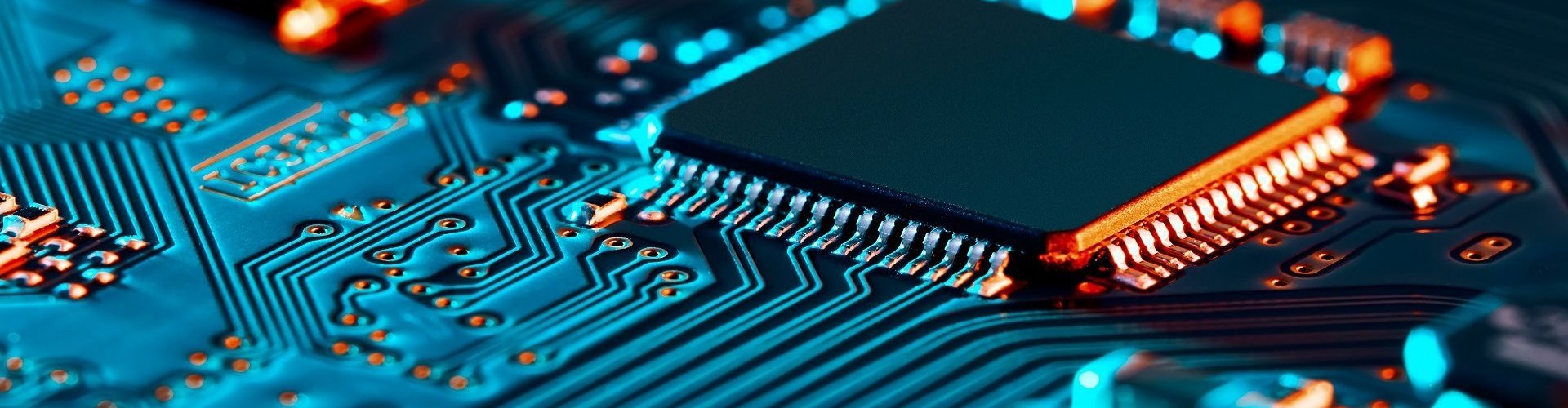
SemiconductorX > Fab & Assembly > Processes & Consumables
Fab Processes & Consumables
An EUV scanner is useless without photoresist flowing onto the wafer at ±0.05°C dispense temperature. A plasma etch chamber is inert without the specialty gases that form the reactive species. A CMP tool polishes nothing without the slurry that provides the chemistry and the pad that provides the mechanics. This sub-pillar catalogs what the equipment consumes and how those consumables behave during the transformation.
Most consumables also appear in Materials & IP, through a different lens: that pillar answers where it comes from and who controls its supply. This sub-pillar answers how it behaves at the point of use — dispense tolerances, interaction with equipment and with the wafer surface, and qualification lock-in with the process flow. Same entities, complementary lenses.
The Six Consumable Categories
Semiconductor manufacturing consumes six major categories of non-equipment materials during the in-process transformation. Each flows continuously into the fab, each has specific dispense and handling requirements at the point of use, and each participates in specific process modules.
| Category | In-Process Role | Point of Use |
|---|---|---|
| Process Gases | Form reactive species in plasma etch, deposit films in CVD and ALD, clean chambers after process cycles, create controlled atmospheres for thermal processing | Gas cabinet systems, mass flow controllers, point-of-use delivery to each process tool; bulk gases via on-site air separation, specialty gases via cylinder or tube trailer |
| Process Chemicals | Wet etch acids (HF, phosphoric, sulfuric) and bases (KOH, TMAH); photoresist developers and rinse chemicals; cleaning solvents and resist strippers; RCA cleaning chemistries; electroplating chemistries for damascene copper | Wet benches, spray tools, track tool developer modules, electroplating cells; single-wafer and batch processing across FEOL, MEOL, and BEOL modules |
| Photoresist & Ancillaries | Photoresist receives the lithographic pattern via UV or EUV exposure; anti-reflective coatings suppress substrate reflection; top-coats and protection layers enable immersion and EUV | Track tool (coater/developer) — paired with every lithography scanner; temperature-controlled dispense at ±0.05°C for EUV |
| CMP Slurries & Pads | Chemical mechanical planarization requires both the chemistry of the slurry (colloidal silica, ceria, or alumina-based) and the mechanics of the polishing pad; planarization enables multi-layer stacking | CMP tools at the end of every metal interconnect deposition cycle — 15+ times per 5nm chip; continuous slurry flow during polish, pad dressing between wafers |
| Sputtering Targets | High-purity metal disks eroded by ion bombardment in PVD tools to deposit copper, aluminum, tungsten, titanium, tantalum, cobalt, and ruthenium films; targets are consumed at predictable rates and replaced on qualification schedules | PVD chambers at metal deposition steps in BEOL and barrier/liner applications |
| Silicon & Compound Wafers | The substrate that becomes the finished chip — consumed in the sense that each wafer is either successful production or yield loss; substrate characteristics (crystal quality, flatness, edge profile, epi layer) govern downstream yield | Wafer load port at the start of the process flow; FOUP-based automation through every tool |
The Process Flow Context
Consumables do not enter the fab as isolated inputs — they enter in the context of specific process flows that determine dispense behavior, interaction with the wafer surface, and qualification requirements. A single leading-edge chip experiences roughly 1,000 process steps across 90 mask layers, with consumable interaction patterns that repeat at different scales throughout the manufacturing cycle.
| Process Flow Segment | Primary Consumables Consumed | In-Process Characteristics |
|---|---|---|
| FEOL — Front-End of Line | Photoresist and developers (every lithography step); process gases (silane, ammonia, fluorocarbons, HBr, dopant gases); wet etch acids (HF, phosphoric) and bases (KOH, TMAH); RCA cleaning chemistries; resist strippers; target materials for gate stack and spacer deposition | Highest lithography precision; most demanding photoresist performance (EUV resist at leading nodes); tightest CD uniformity and overlay tolerances |
| MEOL — Middle-End of Line (Contact Module) | Tungsten precursors (WF6); cobalt, ruthenium, and titanium for contact barriers and liners; CMP slurries tuned for tungsten and cobalt planarization | Metal contact formation with tight resistivity targets; emerging backside power delivery shifts work into this module; CMP is critical for contact uniformity |
| BEOL — Back-End of Line (Interconnect) | Copper sputtering targets; copper electroplating chemistries for damascene fill; low-k dielectric precursors; CMP slurries specific to copper damascene; dielectric etch gases; diffusion barrier materials (Ta, TaN); photoresist and developers for each metal layer | Each metal layer is its own full consumable cycle; BEOL accounts for roughly half of total process steps and a significant share of consumable volume |
| Chamber Clean & Maintenance | NF3 for fluorine-based chamber cleans; SF6 and PFCs for specialty applications; purge gases (N2, Ar) | NF3 is consumed continuously for chamber cleaning between wafers; no-stockpile hazmat classification and high GWP (17,000) make it a distinct supply chain pressure point |
| Advanced Packaging | Solder bumps (SnAg, copper pillar); underfill materials; ABF laminate for organic substrates; glass substrate materials (emerging); TIM (thermal interface materials); mold compound; wire bond wire (copper, gold) | Packaging-specific consumables with different suppliers than front-end; ABF near-sole-source (Ajinomoto Fine-Techno) is a bottleneck distinct from front-end chokepoints |
Qualification Lock-In
Every consumable on every tool at every process node at every fab is qualified. Switching a supplier triggers full re-qualification — 12–24 months for photoresist at leading nodes, comparable for precursor gases, slurries, and wet chemistries. The upstream supply-chain view lives in Materials & IP; the in-process integration view lives here and on the category pages below.
Cross-Pillar Context
Most consumables appear both here and in Materials & IP, through complementary lenses — supply chain upstream, in-process integration here. Consumable handling infrastructure (bulk gas delivery, chemical distribution, UPW) lives in Fab OPS.
Process Gases | Process Chemicals | Photoresist | CMP Slurries | Sputtering Targets | Silicon Wafers | Fab Equipment | Fab Facilities | Fab OPS | Materials & IP | Fab & Assembly Hub